
MIT Develops Ultrafast X-ray Thermometry Method to Observe Heat Transfer in Multilayer Chip Structures
 Scan to share
Researchers at the Massachusetts Institute of Technology (MIT) have developed a new method for observing how heat transfers through multilayer materials, which can be used to precisely measure heat flow variations inside electronic devices such as computer chips. The findings have been published in Nature Communications.
As computer chips continue to shrink in size and power density keeps rising, device overheating has become a major factor limiting performance improvements. Traditional heat flow measurement methods face limitations when dealing with the multilayer structures of real electronic devices—for example, the commonly used time-domain thermoreflectance method struggles to distinguish heat transport in different material layers, while infrared imaging and other approaches also fail to capture rapid changes at microscopic scales.
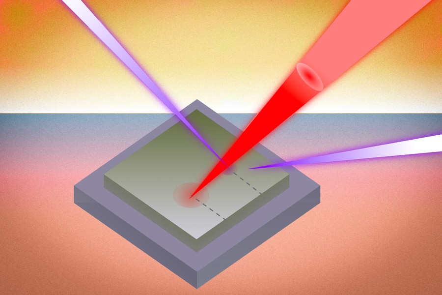
To address this issue, the research team combined laser pulses with ultrafast X-rays: the laser is used to heat the sample, while the X-rays penetrate multiple material layers and scan them, recording internal changes in the material during heat diffusion through signals such as diffraction. The researchers stated that this method enables observation of heat flow distribution at extremely small scales, helping to directly analyze the impact of interfaces and defects on heat dissipation.
The team applied this technique to a test device consisting of a silicon substrate and a gallium nitride layer. Gallium nitride, due to its favorable thermal conductivity potential, is considered suitable for applications such as transistors and flexible electronic devices. Experiments revealed that micron-scale wrinkle defects in the device significantly weaken local heat dissipation capability: thermal conductivity at the defect sites is reduced by approximately fourfold, and the overall heat dissipation capacity of the material decreases by about 25%. The study also showed that such defects cause directional differences in heat diffusion, making heat flow more inclined to propagate along specific directions.
The researchers believe this finding indicates that using only an "ideal defect-free crystal" model may be insufficient to reflect real conditions when simulating heat dissipation in electronic devices. By directly observing the impact of microscopic defects on heat flow, this method can provide experimental evidence for chip thermal design, device structure optimization, and the development of high-power-density electronic products.
The research team stated that this measurement technique is expected to be extended to more material and device systems in the future, for analyzing heat dissipation issues in electronic devices used in applications such as artificial intelligence computing, wearable devices, and clean energy systems. This work was partially supported by the U.S. Department of Energy, the National Science Foundation, and relevant projects at the MIT School of Engineering.
Disclaimer: Information republished from partner media, institutions or other websites is provided for reference and communication purposes only. It does not imply endorsement of its views or verification of its accuracy. Please contact us if any content infringes rights or requires correction.