
Tescan Launches MIRA XR Ultra-High-Resolution Scanning Electron Microscope for Materials Characterization and Failure Analysis Applications
 Scan to share
Tescan recently launched the MIRA XR ultra-high-resolution scanning electron microscope system, targeting materials characterization needs in fields such as battery technology, metallurgy, and advanced materials science. Positioned between the Tescan MIRA and Tescan CLARA, the system aims to deliver higher resolution, enhanced surface sensitivity, and a more streamlined workflow, serving applications including R&D laboratories, industrial quality control, and failure analysis.
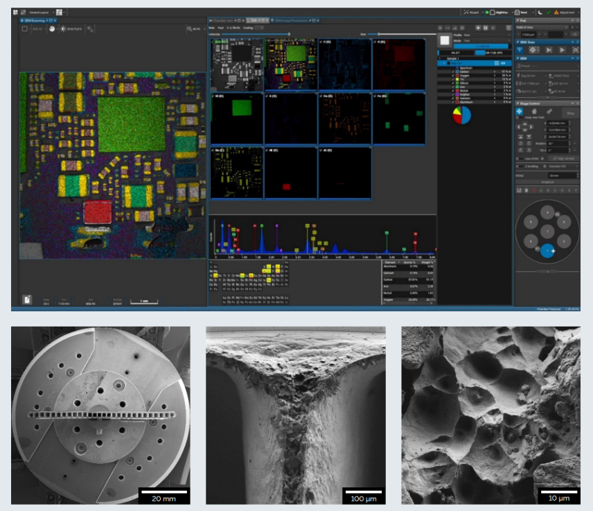
According to reports, the MIRA XR employs BrightBeam™ technology and a single high-efficiency axial detector to improve surface signal acquisition under field-free imaging conditions, making it suitable for beam-sensitive materials and magnetic samples while reducing the need for sample preparation steps such as surface coating. The system also features an aperture-free column design that minimizes manual aperture selection and adjustment steps, allowing operators to focus more on sample observation and data analysis.
In terms of automation, the MIRA XR integrates the In-Flight™ automatic control function, which automatically optimizes key imaging parameters such as focus, astigmatism, and beam alignment. The system also incorporates the Dual Essence™ EDS elemental analysis solution, enabling users to perform real-time compositional mapping within the same SEM operating interface, reducing workflow interruptions caused by switching between different platforms. According to documentation, this integrated workflow can reduce laboratory analysis time by up to 30%.
The application scope of the MIRA XR covers metallurgical defect analysis, fracture analysis, battery materials research, and nanomaterials characterization. In the metallurgical field, the system can be used to identify material defects such as inclusions, voids, and microcracks, and to conduct high-resolution observation of welds, coatings, and bulk materials; in fracture analysis, it helps researchers observe failure features such as fatigue striations, brittle fracture, and ductile fracture.
In battery research, the MIRA XR can be used to analyze ion-milled electrode materials, distinguishing micron-scale cracks and nanoscale defects in cathode materials, and supports morphological analysis of pristine cathode and anode powders. For nanomaterials research, the system can observe features below 10 nanometers at low landing voltages while maintaining high contrast and dimensional accuracy with reduced impact from sample coating.
Tescan stated that the MIRA XR adopts a modular design, offering headroom for future expansion of detectors, automation features, and software capabilities, and can adapt to the demands for high-resolution imaging, rapid analysis, and long-term scalability in scientific research, R&D, and production environments.
Disclaimer: Information republished from partner media, institutions or other websites is provided for reference and communication purposes only. It does not imply endorsement of its views or verification of its accuracy. Please contact us if any content infringes rights or requires correction.