
Gallium ion FIB-SEM sample preparation has a damage limit; low-energy argon ion beam cleaning is used to improve TEM sample quality
 Scan to share
Gallium ion focused ion beam-scanning electron microscopy (Ga⁺ FIB-SEM) has become an important method for site-specific thin lamella sample preparation for transmission electron microscopy/scanning transmission electron microscopy (TEM/STEM), enabling cutting, extraction, and thinning of target regions at the nanometer scale. However, the literature indicates that while gallium ions provide high-precision machining capability, they also cause amorphization, ion implantation, and localized chemical modification on the sample surface, which can subsequently affect high-resolution imaging and energy dispersive spectroscopy analysis results.
According to the literature, Ga⁺ FIB-SEM typically enables high-resolution site-specific machining at 30 keV, but high-energy gallium ions form a damage layer on the sample sidewalls. Taking silicon as an example, existing data indicate that 30 keV Ga⁺ milling can create an amorphous layer approximately 22 nm thick on each side of the lamella. For high-quality STEM samples where the total thickness needs to be controlled below approximately 50 nm, this means that a considerable portion of the sample region may have been altered by the preparation process, particularly affecting atomic-resolution imaging, EDS, EELS, layered interfaces, thin films, grain boundaries, and semiconductor microstructures.
Reducing the Ga⁺ energy can mitigate the damage, for example by using 5 keV or 2 keV for final polishing, but the literature suggests that this does not completely eliminate the implantation, amorphization, and chemical effects introduced by gallium ions as the final machining species. Therefore, low-energy Ar⁺ gentle ion beam cleaning is employed as the final surface treatment after FIB-SEM sample preparation. Argon is a chemically inert element with a shallower interaction depth at low energies; when the energy is below approximately 500 eV, its collision cascade is mainly confined to the near-surface region, enabling layer-by-layer removal of the outer damage layer formed by Ga⁺ machining while avoiding the deep damage and chemical reactions introduced by gallium ion processing.
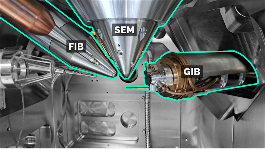
The literature also mentions that the Aura™ Gentle Ion Beam solution integrates low-energy broad-beam Ar⁺ polishing into the FIB-SEM workflow, allowing the sample to undergo final cleaning after Ga⁺ site-specific preparation without the need for transfer to a separate polishing instrument. This approach reduces the risks of sample transfer, contamination, alignment errors, and lamella loss, while improving repeatability through recipe-based operation and in-system quality control.
From a technical perspective, Ar⁺ cleaning does not replace Ga⁺ FIB-SEM but rather complements its final preparation step: Ga⁺ remains responsible for precise positioning and lamella shaping, while low-energy Ar⁺ serves to remove surface preparation damage and improve sample cleanliness and reliability. For sensitive samples such as aluminum alloys, copper, germanium, gallium-containing semiconductors, thin films, multilayer structures, and interface materials, this difference may directly determine the credibility of the final S/TEM analysis results.
Disclaimer: Information republished from partner media, institutions or other websites is provided for reference and communication purposes only. It does not imply endorsement of its views or verification of its accuracy. Please contact us if any content infringes rights or requires correction.