
Korean Research Team First to Quantitatively Reveal Radiation Degradation Mechanisms in Gallium Arsenide Semiconductors
 Scan to share
A semiconductor research team in Korea has recently succeeded, for the first time in the country, in quantitatively identifying the performance degradation mechanisms of gallium arsenide (GaAs) compound semiconductors under radiation environments. Gallium arsenide is regarded as a key material for next-generation aerospace, aviation, and defense systems, and the findings contribute to understanding the impact of high-energy radiation on the reliability of compound semiconductor devices.
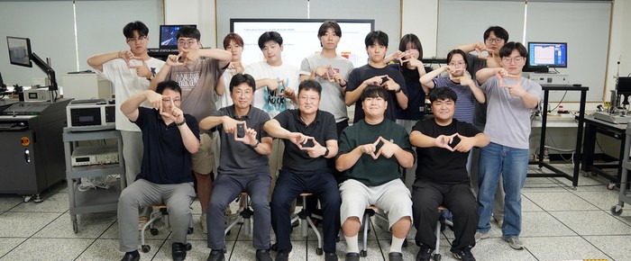
The research was led by Professor Kim Min-soo and Professor Hwang Hyun-jun from the Department of Semiconductor Engineering, in collaboration with the Advanced Radiation Research Center at the Korea Atomic Energy Research Institute and WaveTrack Corporation. The research team noted that communication and power equipment aboard low-Earth-orbit satellites or detectors, when exposed to high-energy radiation environments over extended periods, may experience performance degradation or even failure. This study is the first to clearly elucidate the changes in passive components within compound semiconductors under radiation conditions. Compared with traditional silicon materials, compound semiconductors offer advantages such as higher speed and greater voltage tolerance, making their radiation reliability critically important for future aerospace and defense electronic systems.
In addition to semiconductor reliability research under radiation environments, the college continues to advance the translation of research outcomes into practical applications in related frontier fields. For example, a paper by Professor Kang Jang-won and Professor Song Jung-hun's team on quantum dot thin films was selected as a cover article for an international academic journal. These research outcomes are being incorporated into student capstone design projects and undergraduate research programs to cultivate talent for next-generation technology development.
Currently, the Compound Semiconductor Center under the Department of Semiconductor Engineering is providing Korea's first compound semiconductor multi-project wafer (MPW) service. Mokpo National University is responsible for the final reliability verification of the MPW process, promoting a greater role for South Jeolla Province and Gwangju in the compound semiconductor industry landscape. The service also provides Korean startups, university laboratories, and small and medium-sized enterprises with direct opportunities to design and manufacture new compound semiconductor chips.
Meanwhile, the center is collaborating with companies such as Taiwan's Win Semi, America's Amkor Technology, and Keysight Technologies to build a full-cycle semiconductor development system covering design, manufacturing, and packaging. These developments are expected to help Korea further enhance its competitiveness in next-generation defense and aerospace semiconductors, beyond memory semiconductors.
Disclaimer: Information republished from partner media, institutions or other websites is provided for reference and communication purposes only. It does not imply endorsement of its views or verification of its accuracy. Please contact us if any content infringes rights or requires correction.