
Singapore team develops deuterated silicon nitride waveguides for wafer-scale broadband light generation
 Scan to share
A research team from the Singapore University of Technology and Design and the Institute of Microelectronics at the Agency for Science, Technology and Research (A*STAR) in Singapore has recently developed a low-loss deuterated silicon nitride waveguide capable of on-chip broadband light generation. By replacing hydrogen with its heavier isotope deuterium, the team fabricated silicon nitride waveguides at low temperatures, demonstrating potential for integration with CMOS-compatible semiconductor processes and wafer-scale mass production. Traditionally, silicon nitride thin films are grown from silane gas, and residual silicon-hydrogen bonds in the material absorb light in the telecommunications band, requiring high-temperature annealing that is incompatible with integrated electronic circuits.
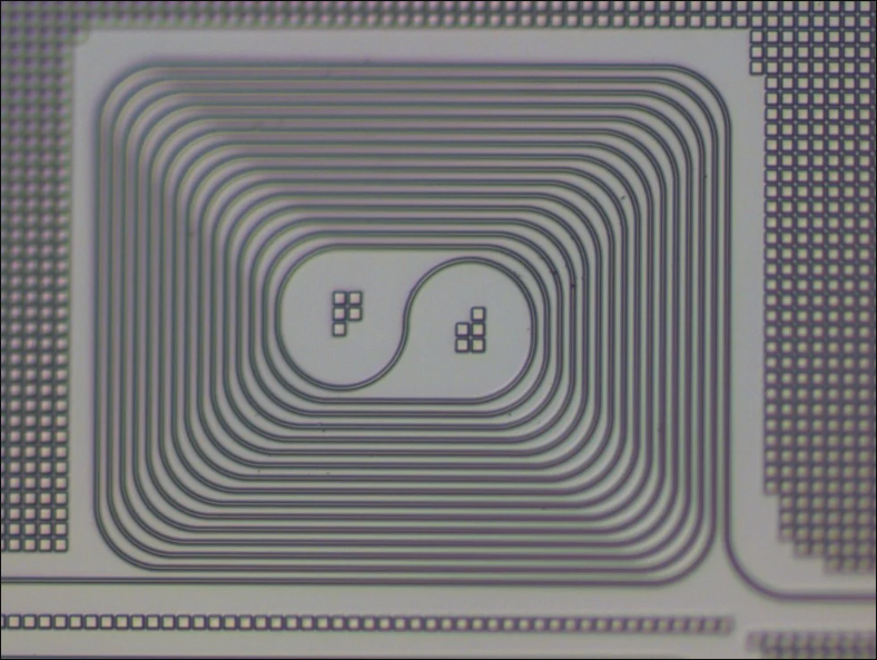
The related paper, "Octave-spanning supercontinuum generation in wafer-scale low-loss deuterated silicon nitride waveguides," was published in *Optics Letters*. The study shows that this chip-scale waveguide can broaden infrared laser pulses to cover a spectral range from visible red light to deep infrared.
Conventional silicon nitride thin films are typically grown from silane gas, and residual silicon-hydrogen bonds in the material absorb light in the telecommunications band. To reduce absorption, conventional processes require prolonged annealing at temperatures as high as 1200 degrees Celsius, but such high-temperature treatments are incompatible with chips that already have integrated electronic circuits and can also introduce significant stress in thick films.
The research team instead used deuterated silane in place of standard silane, replacing hydrogen atoms with the heavier deuterium isotope. Dawn Tan, Associate Professor at the Singapore University of Technology and Design, stated that this substitution shifts the absorption peak from the communications band to the 2.1-micrometer region, so light at the operating wavelength is no longer significantly absorbed, eliminating the need for high-temperature baking processes.
According to the team, the process can deposit an 800-nanometer-thick film on an entire 8-inch wafer in a single step at temperatures below 400 degrees Celsius, meeting the thermal budget requirements of standard semiconductor production lines. The fabricated waveguides exhibit an optical loss of 0.54 dB per centimeter and can support high-intensity optical interactions. Devices demonstrated in the study include a waveguide with a length of 5.21 centimeters, as well as a deuterated silicon nitride waveguide with a length of 1.51 centimeters, a spiral layout, and a bend radius of 100 micrometers.
In experiments, after inputting 500-femtosecond infrared pulses into the waveguide, the researchers observed the spectrum broaden from a narrow line at 1555 nanometers to a continuous spectrum spanning from 587 nanometers to 1883 nanometers, covering 1.7 octaves. Although the input light was invisible infrared, the chip emitted visible red light. Tan noted that this demonstrates the device's ability to effectively convert infrared input into a sufficiently broad spectrum extending into the visible range.
For applications such as precision metrology and frequency combs, coherence and pulse-to-pulse stability are as important as spectral width. The team measured an overall spectral coherence above 0.81 at moderate pulse energies, indicating good pulse-to-pulse stability. However, at higher energies, further spectral broadening is accompanied by increased noise, attributed to modulation instability effects. Simulation results suggest that optimizing waveguide length could capture a stable broad spectrum before coherence degrades significantly.
Luo Xianshu, head of the Silicon Photonics Department at the Institute of Microelectronics, A*STAR, noted that the key challenge lies in translating photonic designs into processes that can achieve target optical performance at wafer scale. The research team stated that next steps include optimizing waveguide designs to improve spectral uniformity and broad spectral range at high power, as well as exploring integration of the light source with components such as modulators and detectors on a single chip, targeting applications in medical imaging, precision metrology, and optical communications.
Disclaimer: Information republished from partner media, institutions or other websites is provided for reference and communication purposes only. It does not imply endorsement of its views or verification of its accuracy. Please contact us if any content infringes rights or requires correction.