
German BESSY II Research Reveals: Cesium Chloride Seed Layer Can Improve Quality of Perovskite-Silicon Tandem Solar Cells
 Scan to share
A team from the Helmholtz-Zentrum Berlin (HZB) in Germany used the BESSY II synchrotron radiation facility to conduct nanoscale analysis of perovskite-silicon tandem solar cells fabricated by evaporation methods, and proposed a new approach to improve the quality of perovskite thin films. The study shows that introducing a thin cesium chloride (CsCl) seed layer between the two sub-cells promotes uniform growth of the perovskite layer while reducing undesirable lead iodide deposition at the interface.
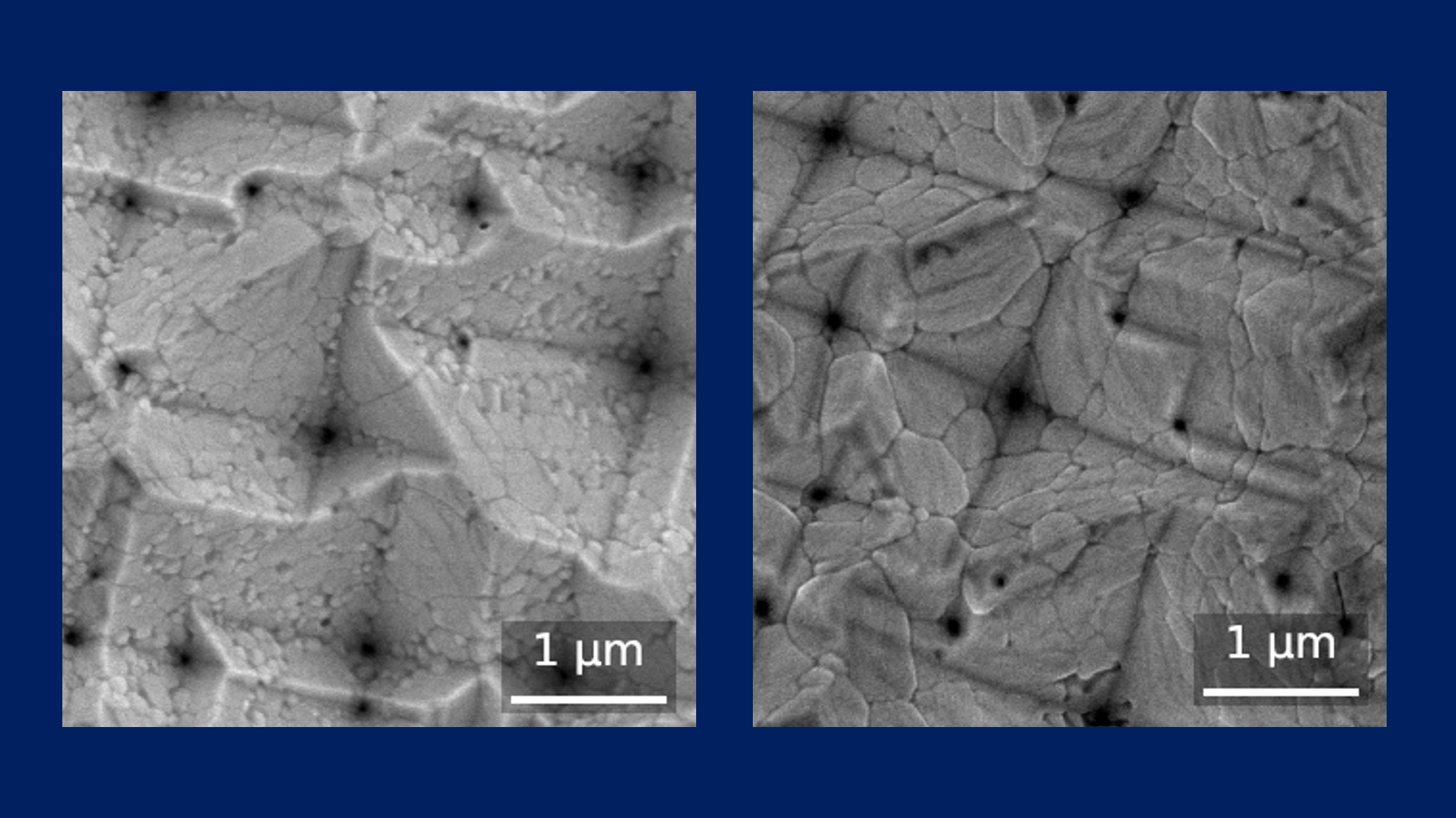
The research demonstrates that the cesium chloride seed layer improves the growth of the evaporated perovskite layer and reduces the formation of lead iodide. Scanning electron microscopy images show that the perovskite layer grown without a seed layer (left image) consists of extremely fine grains with numerous defects, while the perovskite layer grown on the cesium chloride seed layer (right image) exhibits significantly larger grains and markedly fewer defects. HZB
Perovskite-silicon tandem solar cells typically achieve higher conversion efficiencies than single-junction silicon solar cells. Among the fabrication routes, co-evaporating perovskite precursor molecules onto the silicon sub-cell is an industrially attractive approach. The research team noted that such monolithic tandem cells typically require a self-assembled monolayer (SAM) on the silicon surface to serve as the hole transport layer, but both the SAM layer and the perovskite layer must cover the silicon surface as uniformly as possible. Since the SAM is not a perfect monolayer and the silicon surface often features nanotextured structures for enhanced light trapping, achieving uniform film formation is not straightforward.
At BESSY II, the researchers employed infrared near-field scanning probe microscopy (IR-s-SNOM) to identify regions within the SAM layer with varying thicknesses, including monolayers, multilayers, and areas of SAM molecular aggregation. Further analysis revealed that on both planar silicon substrates and industrially relevant textured silicon substrates, SAM molecules tend to aggregate at the bottom of texture valleys, resulting in non-uniform film thickness.
Subsequently, the team used X-ray photoemission electron microscopy (XPEEM) at BESSY II to observe the growth of co-evaporated perovskite on different SAM-covered regions. The results showed that the perovskite layer cannot compensate for the non-uniformity of the underlying SAM layer and tends to form undesirable lead iodide at the interface with silicon.
To address this issue, the researchers introduced a cesium chloride layer at the interface to serve as a seed layer. Dr. Viktor Škorjanc, first author of the study, stated that this seed layer enables more uniform growth of the perovskite film on textured silicon surfaces and helps avoid interfacial defects caused by non-uniform coverage of the hole transport layer. Scanning electron microscopy observations also confirmed that without the seed layer, the perovskite film exhibits smaller grains and more defects; with the cesium chloride seed layer, film defects are significantly reduced and grain size increases.
The research results show that with this approach, the perovskite-silicon tandem solar cell achieved an efficiency of 30.3%. Dr. Marcel Roß, head of the evaporated perovskite solar cell team at HZB, noted that this solvent-free vacuum process also holds promise for improving tandem cell stability, which is of great significance for advancing high-efficiency laboratory results toward reliable, industrially producible tandem solar technologies.
Disclaimer: Information republished from partner media, institutions or other websites is provided for reference and communication purposes only. It does not imply endorsement of its views or verification of its accuracy. Please contact us if any content infringes rights or requires correction.