
U.S. Research Team Discovers Strong Ultrafast Optical Response Induced by Ionizing Radiation, Potentially Advancing Medical Imaging and Sensing Technologies
 Scan to share
September 3 news, Stanford University and the U.S. Department of Energy's SLAC National Accelerator Laboratory research team used ultrafast electron and laser pulses to observe a strong ultrafast optical response triggered by ionization processes in semiconductor materials. The related research has been published in Nature·Photonics. The researchers believe this discovery could provide new insights for radiography and sensing technologies, and also offer experimental evidence for understanding the fundamental behavior of materials under high-energy particle interactions.
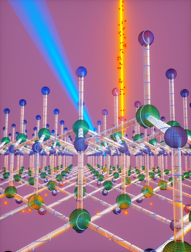
Radiation detection is a key technology in particle accelerators, scientific instruments, medical imaging, and security screening equipment. Existing detectors typically face a trade-off between signal strength and response speed: detection processes with stronger signals tend to be slower, while those with faster response may produce weaker signals. This limitation can affect detection accuracy and real-time imaging capabilities.
In this study, the team conducted experiments using the megaelectronvolt ultrafast electron diffraction (MeV-UED) facility at SLAC's Linac Coherent Light Source. This system is typically used as an "electron camera" for studying atomic and molecular dynamics, but in this work, the researchers did not use electrons to image samples. Instead, they injected high-energy electrons into semiconductor samples to simulate ionization processes in applications such as positron emission tomography (PET), and then used synchronized ultrafast laser pulses at different wavelengths to probe the optical changes in the material immediately after ionization.
The research subjects were II-VI semiconductors, a class of materials commonly used in electronic applications such as infrared detectors and photovoltaic solar cells. Experimental results showed that the research team not only obtained strong ultrafast radiation-related signals but also observed that the distribution of charge carriers within the material differed from expectations. The researchers had originally anticipated that electron-hole pairs generated by high-energy electrons would be relatively uniformly dispersed throughout the sample; however, actual observations revealed that these charge carriers tend to cluster in localized high-density regions.
This localized dense charge distribution alters the material's bandgap—the energy range in which no electronic states exist in the material—thereby affecting how the semiconductor absorbs and transmits light. The researchers reported that under high-energy electron excitation, the semiconductor exhibited a significant bandgap energy shift, causing it to transmit light under conditions where it would normally be opaque.
The research team believes that understanding how high-energy electrons form localized high-energy regions in materials and produce strong optical signals will aid in developing new sensing platforms. The related effects could potentially be applied in lower-energy imaging systems in the future, such as real-time imaging and disease diagnostic technologies in medical settings. The researchers expressed hope that this direction could ultimately support rapid imaging and real-time intervention applications. The study was funded by the U.S. Department of Energy Office of Science, the National Science Foundation, and the National Institutes of Health, among others.
Disclaimer: Information republished from partner media, institutions or other websites is provided for reference and communication purposes only. It does not imply endorsement of its views or verification of its accuracy. Please contact us if any content infringes rights or requires correction.